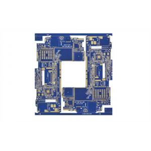
Blue BGA Rigid PCB Board High TG180 2 OZ Copper Thickness 1.6MM Board Thickness
Number of layers: 2 layers
Material: FR4
Board thickness: 1.6mm
Surface plating: ENIG
Special process description: 2OZ
Solder mask: Blue
With 13+ years of PCB manufacturing experience in the China, and 10+ years of experience exporting PCBs overseas, We understands the needs of your business and welcomes the opportunity to serve you.
Our dedication to building a quality product is the centerpiece of our business policy.
We are committed to fulfilling our customers' on-going quality requirements through continuous improvements to all of our internal processes. Our quality management system ensures the highest operating standards at all levels.
Please call GSC if you need:
Fast turn-around prototypes.
Low-Medium-High volume production requirements.
To meet your prodution schedules.
On time delivery with a quality product.
A competitive price
PROTOTYPE AND VOLUME PRODUCTION:
Single sided
Double sided
Multilayer up to 8 layers
Immersion white tin process
For PCBA order, provide us:
- PCB Gerber file
- BOM list for PCBA
- Sample of PCB and PCBA
- Test method for PCBA
Services and applications:
- Through hole board assembly
- SMT assembly including BGA assembly, smallest placement: 0201
- Material procurement
- Consigned material management
- Plastic or metal enclosure
- Complex final assembly
- Functional test
- Cable assembly
- Labeling and packing
- Customized logistics per customer
- Laser cut framed SMT solder paste stencils
- PCB design and schematic capture
Competitive advantages:
- No minimum order quantity and free sample
- Focus on low to medium volume production
- Quick and on-time delivery
- International approvals
- Great customer service
- Diversified shipping method
| Materials | Standard | Advanced |
| FR4 (130‐180 Tg by DSC) | Y | Y |
| Halogen Free | Y | Y |
| BT Epoxy | Y | Y |
| Getek | Y | Y |
| Isola 370HR 406 408 IS410 IS 420 IS620 | Y | Y |
| Nelco 4000 | Y | Y |
| Rogers 4000 | Y | Y |
| PTFE | Y | Y |
| Dupont Pyralux | N | Y |
| Aluminum Core | Y | Y |
| Surface Finishes |
| ENIG | Y | Y |
| Flash Gold | Y | Y |
| Electrolytic Nickel/Hard Gold | Y | Y |
| HASL | Y | Y |
| Lead Free HASL | Y | Y |
| Immersion Ag | Y | Y |
| Standard Features | Standard | Advanced |
| Maximum layer count | 20 | 36 |
| Maximum Panel Size | 21″x24″ | 24″x30″ |
| Outer Layer Trace/Spacing (1/3 oz) | 0.0035″/0.0035″[90μm/90μm] | 0.0025″/0.003″[64μm/76μm] |
| Inner Layer Trace/Spacing (H oz) | 0.003″/0.003″ [76μm/76μm] | 0.002″/0.0025″ [50μm/64μm] |
| Maximum PCB thickness | 0.125″[3.2mm] | 0.177″[4.5mm] |
| Minimum PCB thickness | 0.008″[0.20mm] | 0.004″[0.10mm] |
| Minimum mechancial drill size | 0.008″[0.20mm] | 0.004″[0.10mm] |
| Maximum PCB aspect ration | 10:01 | 12:01 |
| Maximum copper weight | 5 oz [178μm] | 6 oz [214μm] |
| Minimum copper weight | 1/3 oz [12μm] | 1/4 oz [9μm] |
| Minimum core thickness | 0.002″[50μm] | 0.0015″[38μm] |
| Minimum dielectric thickness | 0.0025″[64μm] | 0.0015″[38μm] |
| Minimum Pad Size over Drill | 0.018″[0.46mm] | 0.016″[0.4mm] |
| Solder Mask Registration | +/‐ 0.002″[50μm] | +/‐ 0.0015″[38μm] |
| Mimimum Solder Mask Dam | 0.003″[76μm] | 0.0025″[64μm] |
| Copper feature to PCB edge | 0.015″[0.38mm] | 0.010″[0.25mm] |
| Tolerance on overall dimensions | +/‐ 0.004″[100μm] | +/‐ 0.002″[50μm] |
| HDI Features |
| Immersion Tin | Y | Y |