Add to Cart
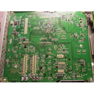
HASL Multilayer Green PCB Board FR4 PCB Assembly TG 150 1.5mm Thickness
High quality Multilayer GREEN FR4 PCB assembly 0201 / PCB manufacturer in China
Number of layers: 2 layers
Material: FR4
Board thickness: 1.5mm
Surface plating: HASL
Copper thickness :2OZ
Special process description: TG150
Quality System Standards
ISO 9001:2008 certified.
Acceptability Criteria
IPC-A-600 (Latest Revision) class 2 and 3
Performance Specification
IPC-A-6012 (Latest Revision) class 2 and 3.
UL 796,94V-0
Certifications and Reports Available
Base Laminates to IPC-4101
Microsection Evaluation
Thermal Stress Evaluation
Electrical Test to IPC-9252
Ionic Contamination to IPC-6012
Solderability to J-STD-003
Xray Flurescence and Capacitancne Plating Thickenss
EDAX, SEM by request
Impedance
PCBA/PCB assembly specifications:
What can we do for you?
For PCBA order, provide us:
Services and applications:
PCBA capabilities:
Competitive advantages:
| Item | Mass production | Small batch production | ||
| Number of layers | UP TO 18L | UP TO L | ||
| Laminate type | FR-4, halogen free, high TG(Shengyi, KB), Cem-3, PTFE, aluminum based, PTEE, Rogers or more. | FR-4, Halogen free, High TG(Shengyi, KB), Cem-3, PTFE, Aluminum based, PTEE, Rogers or more. | ||
| Maximum board size | 610mm*1100mm | 610mm*1100mm | ||
| Board thickness | 0.1mm-7.00mm | <0.1mm and >7.00mm | ||
| Minimum line width/space | 3.5mil(0.0875mm) | 3mil(0.075mm) | ||
| Minimum line gap | +/-15% | +/-10% | ||
| Outer layer copper thickness | 35um-175um | 35um-210um | ||
| Inner layer copper thickness | 12um-175um | 12um-210um | ||
| Drilling hole size(Mechanical) | 0.15mm-6.5mm | 0.15mm-6.5mm | ||
| Finished hole size (Mechanical) | 0.15mm-6.0mm | 0.15mm-6.0mm | ||
| Board thickness hole size ratio | 14:1 | 16:1 | ||
| Board thickness tolerance(t=0.8mm) | ±8% | ±5% | ||
| Board thickness tolerance(t<0.8mm) | ±10% | ±8% | ||
| Min. grid line width | 4mil(12, 18, 35um), 6mil(70um) | 4mil(12, 18, 35um), 6mil(70um) | ||
| Min. grid spacing | 6mil(12, 18, 35um), 8mil(70um) | 6mil(12, 18, 35um), 8mil(70um) | ||
| Hole size tolerance(Mechanical) | 0.05-0.075mm | 0.05mm | ||
| Hole position tolerance(Mechanical) | 0.005mm | 0.005mm | ||
| Solder mask color | Green, Blue, Black, White, Yellow, Red, Grey etc. | Green, Blue, Black, White, Yellow, Red, Grey etc. | ||
| Impedance control tolerance | +/-10% | +/-8% | ||
| Min. distance between drilling to conductor(non-blind buried orifice) | 8mil(8L), 9mil(10L), 10mil(14L), 12mil(26L) | 6mil(8L), 7mil(10L), 8mil(14L), 12mil(26L) | ||
| Min. Character width and height(35um base copper) | Line width: 5mil Height: 27mil | Line width: 5mil; height: 27mil | ||
| Max. test voltage | 500V | 500V | ||
| Max. test current | 200mA | 200mA | ||
Surface treatment | Flash Gold | 0.025-0.075um | 0.025-0.5um | |
| Immersion Gold | 0.05-0.1um | 0.1-0.2um | ||
| Sn/Pb HASL | 1-70um | 1-70um | ||
| Lead-free HASL | 1-70um | 1-70um | ||
| Immersion Silver | 0.08-0.3um | 0.08-0.3um | ||
| OSP | 0.2-0.4um | 0.2-0.4um | ||
| Gold Finger | 0.375um | >=1.75um | ||
| Hard Gold Plating | 0.375um | >=1.75um | ||
| Immersion Sin | 0.8um | |||
| V-Cut rest thickness tolerance | ±0.1mm | ±0.1mm | ||
Outline profile | Chamfer | The angle type of the chamfer | 30,45,60 | |
| Plug via hole | Max.size can be plugged | 0.6mm | ||
| Largest NPTH hole size | 6.5mm | >6.5mm | ||
| Largest PTH hole size | 6.5mm | >6.5mm | ||
| Min. solder spacer ring | 0.05mm | 0.05mm | ||
| Min. solder bridge width | 0.1mm | 0.1mm | ||
| Drilling diameter | 0.15mm-0.6mm | 0.15mm-0.6mm | ||
| Min. pad diameter with hole | 14mil( 0.15mm drilling) | 12mil( 0.1mm laser) | ||
| Min. BGA pad diameter | 10mil | 8mil | ||
| Chemical ENIG gold thickness | 0.025-0.1um(1-4U) | 0.025-0.1um | ||
| Chemical ENIG nickel thickness | 3-5um(120-200U) | 3-5um | ||
| Min. resistance test | Ω | 5 | ||

