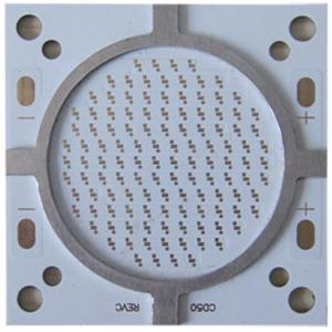
High Power Street Light Single Sided PCB Board Aluminum Base 2 Oz 1 W 2 W 3 W 5 W LEDs
Global Success Circuits is a China printed circuit board manufacturer located in Shenzhen, Jiangxi and Jiangsu. We specialize in the manufacture of 1-18L, fast turnaround bare printed circuit boards.
Just-in-time logistics and delivery are crucial for today's PCB manufacturers. Global Success Group can help your business stay ahead of the competition by improving quality, productivity, and delivery in your supply chain while reducing costs.
With 13+ years of PCB manufacturing experience in the China, and 10+ years of experience exporting PCBs overseas, We understands the needs of your business and welcomes the opportunity to serve you.
| Materials | Standard | Advanced |
| FR4 (130‐180 Tg by DSC) | Y | Y |
| Halogen Free | Y | Y |
| BT Epoxy | Y | Y |
| Getek | Y | Y |
| Isola 370HR 406 408 IS410 IS 420 IS620 | Y | Y |
| Nelco 4000 | Y | Y |
| Rogers 4000 | Y | Y |
| PTFE | Y | Y |
| Dupont Pyralux | N | Y |
| Aluminum Core | Y | Y |
| Surface Finishes |
| ENIG | Y | Y |
| Flash Gold | Y | Y |
| Electrolytic Nickel/Hard Gold | Y | Y |
| HASL | Y | Y |
| Lead Free HASL | Y | Y |
| Immersion Ag | Y | Y |
| Standard Features | Standard | Advanced |
| Maximum layer count | 20 | 36 |
| Maximum Panel Size | 21″x24″ | 24″x30″ |
| Outer Layer Trace/Spacing (1/3 oz) | 0.0035″/0.0035″[90μm/90μm] | 0.0025″/0.003″[64μm/76μm] |
| Inner Layer Trace/Spacing (H oz) | 0.003″/0.003″ [76μm/76μm] | 0.002″/0.0025″ [50μm/64μm] |
| Maximum PCB thickness | 0.125″[3.2mm] | 0.177″[4.5mm] |
| Minimum PCB thickness | 0.008″[0.20mm] | 0.004″[0.10mm] |
| Minimum mechancial drill size | 0.008″[0.20mm] | 0.004″[0.10mm] |
| Maximum PCB aspect ration | 10:01 | 12:01 |
| Maximum copper weight | 5 oz [178μm] | 6 oz [214μm] |
| Minimum copper weight | 1/3 oz [12μm] | 1/4 oz [9μm] |
| Minimum core thickness | 0.002″[50μm] | 0.0015″[38μm] |
| Minimum dielectric thickness | 0.0025″[64μm] | 0.0015″[38μm] |
| Minimum Pad Size over Drill | 0.018″[0.46mm] | 0.016″[0.4mm] |
| Solder Mask Registration | +/‐ 0.002″[50μm] | +/‐ 0.0015″[38μm] |
| Mimimum Solder Mask Dam | 0.003″[76μm] | 0.0025″[64μm] |
| Copper feature to PCB edge | 0.015″[0.38mm] | 0.010″[0.25mm] |
| Tolerance on overall dimensions | +/‐ 0.004″[100μm] | +/‐ 0.002″[50μm] |
| HDI Features |
| Immersion Tin | Y | Y |
PCBA Testing
We equipped a team of 3 skilled technical engineers who have many years experience in the field to put our strict testing flows and standards into practice. In the whole testing flow, by AOI, flying test and testing jig test we first test the flows of circuit board production including through-hole status, short circuit and appearance, etc. For some complicated craft flows e.g. in high precision or blind via boards, even only wafer analysis can discover testing problems.
Our PCBA test is a complete system which includes FCT, ICT, AOI and so on, so that we make sure each product out of our factory are consistent with the designed parameters and specifications. Before the PCB assembly, we always need to communicate with customers for the confirmation of a test plan. Usually our testing team will help our customers copy if they are pleased to hand over IC program, and then make FCT by testing jig which is usually customized according to PCB functions. (For full idea about FCT, ICT and AOI, you may know about them by Google.)
About 1000 workers, 50000 ㎡ workshop, 13 years experience, 10 years' of exporting, ISO, TS & SGS certificated, 3 factories located in Shenzhen, Jiangxi and Jiangsu, this is how we keep superior quality and competitive offers for global valued customers.
Our main service cover PCB and PCB assembly..
If any product meet your demand, please contact us for further information.
We're sure your any inquiry or requirement will get prompt attention.